SI1013R-T1-GE3
| Do pobrania | Download |
|---|---|
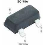
| Main description | Trans MOSFET P-CH 20V 0.35A 3-Pin SC-75A T/R |
Trans MOSFET P-CH 20V 0.35A 3-Pin SC-75A T/R
Informacje podstawowe
- ProducentVishay
- EURoHSYes (2011/65/EU, 2015/863)
- Automotive No
Informacje dodatkowe
- Crosses 35
- Inventory 7
- PCNs 24
- GIDEP-Alerts 1
- MaskPart SI1013R%GE3
- IntroductionDate Oct 27, 2000
Parametry
- Category Power MOSFET
- Channel Mode Enhancement
- Channel Type P
- Configuration Single
- Material N/A
- Maximum Continuous Drain Current (A) 0.35
- Maximum Continuous Drain Current @ Temperature (A) 0.275@Ta=85C
- Maximum Drain Source Resistance (mOhm) 1200@4.5V
- Maximum Drain Source Resistance @ Vgs (mOhm) 1200@4.5V|1600@2.5V|2700@1.8V
- Maximum Drain Source Voltage (V) 20
- Maximum Gate Source Voltage (V) ±6
- Maximum Gate Threshold Voltage (V) 0.45(Min)
- Maximum Junction Ambient Thermal Resistance N/A
- Maximum Junction Case Thermal Resistance N/A
- Maximum Power Dissipation (mW) 175
- Maximum Storage Temperature (°C) 150
- Minimum Storage Temperature (°C) -55
- Number of Elements per Chip 1
- Process Technology TrenchFET
- Supplier Temperature Grade N/A
- Typical Drain Source Resistance @ 125°C (mOhm) N/A
- Typical Drain Source Resistance @ 25°C (mOhm) 800@4.5V|1200@2.5V|1800@1.8V
- Typical Fall Time (ns) 11
- Typical Forward Transconductance (S) 0.4
- Typical Gate Charge @ 10V (nC) N/A
- Typical Gate Charge @ Vgs (nC) 1500@4.5V
- Typical Gate Resistance (Ohm) N/A
- Typical Gate to Drain Charge (nC) 450
- Typical Gate to Source Charge (nC) 150
- Typical Input Capacitance @ Vds (pF) N/A
- Typical Output Capacitance (pF) 13
- Typical Reverse Recovery Charge (nC) N/A
- Typical Rise Time (ns) 9
- Typical Switch Charge (nC) N/A
- Typical Turn-Off Delay Time (ns) 35
- Typical Turn-On Delay Time (ns) 5